RgGen ✕ OpenMPW Walkthrough
Abstract
The motivation of this article is to lower the threshold for participation in OpenMPW, and the method is to generate CSRs with Wishbone interface using RgGen. It’s done, it’s certainly easy, it’s going viral, let’s donate to RgGen, that’s all.
Introduction
Hi, I’m Cra2yPierr0t.
The number of participants in my country in OpenMPW is not increasing very much. I miss it. Well, I can understand why. It is easy to write Verilog (you are a fool if you can’t write Verilog), but there is a mysterious bus protocol called wishbone, OpenLANE configuration is too difficult for integrated circuit amateurs, SRAM needs to be replaced, and so on.
I wrote about SRAM last time, so let’s deal with wishbone next. Yes, with RgGen.
Seeing is believing, and this article introduces the flow of easy LSI design using RgGen.
Prerequisites
About RgGen
RgGen is a CSR generation tool created by Mr. Ishitani (@taichi600730). It can generate CSR with various functions from a configuration file. It is also possible to add a wishbone interface to the CSRs (APB and AXI4-lite are also possible).
What this means is that with RgGen, you are free from having to read the wishbone specification to create the control logic for the wishbone, and from the tedious work of setting some registers to RO and others to RW! I’m very happy about that.
https://github.com/rggen/rggen
About OpenMPW
Shuttle program started by Google, Efabless and Skywater in cooperation, all manufacturing and shipping fees free! You can burn LSI for American money!!!
About Caravel
OpenMPW uses a framework called Caravel. https://github.com/efabless/caravel_user_project
Caravel is divided into MGMT Core and User Project Area. The MGMT Core is the RISC-V core and peripherals area, which is fixed. User Project Area is an area where users can freely handle and insert their own designs.
The MGMT Core and User Project Area are connected by two buses called Wishbone and Logic Analyzer, through which the MGMT Core’s RISC-V core can control your design and send and receive data.
There are also 38 GPIOs extending from the User Project Area to the outside world, through which data can be exchanged with the outside world.
MMIO in Caravel
Caravel’s memory map is as per the following document, allowing the user to work freely in the range 0x3000_0000 to 0x8000_0000-1.
https://caravel-harness.readthedocs.io/en/latest/memory-mapped-io-summary.html
In the following, the base address of CSR is assumed to be 0x3000_0000.
Installing Caravel
I’ll write this down just in case. Download caravel_user_project from here. https://github.com/efabless/caravel_user_project
You can create a repository from template, fork it, or clone it as you like, but if you create a repository from template, updating may be troublesome.
In this case, we will generate and clone from template.
clone git@github.com:<Github ID>/caravel_walkthrough_uart.git
Go into the repository and create a dependencies directory.
cd caravel_user_project
mkdir dependencies
Select the OpenLANE installation location and the PDK to be installed in the environment variable. sky130A will install Skywater’s 130nm and gf180mcuC will install GlobalFoundries’ 180nm PDK. Decide according to the shuttle you want to submit, this time assuming SKY130.
export OPENLANE_ROOT=$(pwd)/dependencies/openlane_src
export PDK_ROOT=$(pwd)/dependencies/pdks
export PDK=sky130A or export PDK=gf180mcuC
Start installation
make setup
What is OpenLANE?
OpenLANE is an OSS RTL to GDSII compiler. OpenLANE itself is a combination of about 20 OSS and is being developed at a very fast pace. https://github.com/The-OpenROAD-Project/OpenLane
What is SKY130 PDK?
SkyWater Technology’s 130nm process PDK. PDK (Process Design Kit) is a collection of information on physical properties of primitive devices such as AND and OR circuits, etc. It is now open source in the name of Google. https://github.com/google/skywater-pdk
What is GF180 PDK?
Global Foundries’ 180nm process PDK. there was the first shuttle, GFMPW-0, last time. https://github.com/google/gf180mcu-pdk
LSI to be created this time
Let’s add a UART to Caravel this time. Actually, UART is already implemented in MGMT Core, but we will ignore it and add our own UART hardware in User Project Area.
The finished product is a RISC-V microcontroller that can send and receive characters via UART.

Note that all the files created in this article have been uploaded to caravel_walkthrough_uart. Please refer to them as needed.
https://github.com/Cra2yPierr0t/caravel_walkthrough_uart
Think about specifications
Now let’s make a policy of what kind of operation we want the LSI to perform.
LSI -> PC: Send when a character is put in the register and a bit is set, and the bit will drop when it is completed.LSI <- PC: Interrupt when a character arrives, read the character and the interrupt bit drops.
This is about right.
Think about what CSR we might need
Next, let’s consider what CSRs are likely to be necessary. Naturally, registers to store receive and transmit data are necessary. In addition, a register to start transmission, an interrupt ON/OFF for reception, and a register to specify the baud rate or operating frequency are necessary since UART has a baud rate. Since it is currently unknown at what MHz the LSI can operate, we will use the register that specifies the operating frequency this time. The baud rate is fixed at 115200.
The table below shows the CSRs we have determined above.
| address | CSR | field | access | Description |
|---|---|---|---|---|
0x3000_0000 |
CLOCK_FREQ |
clock_freq[31:0] |
RW | LSI operating frequency |
0x3000_0004 |
RECEIVED_DATA |
reserved[31:8], rx[7:0] |
RO | received data |
0x3000_0008 |
TRANSMISSION_DATA |
reserved[31:8], tx[7:0] |
RW | transmission data |
0x3000_000c |
INTERRUPT_ENABLE |
reserved[31:1], irq_en[0] |
RW | receive interrupt enabled |
0x3000_0010 |
TRANSMISSION_START |
reserved[31:1], tx_start[0] |
RW | Write 1 to start sending, auto drop on completion |
Note that even simple hardware such as UART requires CSRs with special functions, such as TRANSMISSION_START, which automatically drops bits, and RECEIVED_DATA, which drops interrupt bits after reading a value.
Generate CSR with RgGen
Now let’s create CSR with RgGen referring to the table above.
Installation
Installation of RgGen itself
gem install rggen
Next, install the Verilog plugin for RgGen
gem install rggen-verilog
How to use RgGen
If you want to know how to use RgGen in detail, please go to the main repository. https://github.com/rggen/rggen
RgGen requires two types of input files: the first is a configuration file, which specifies bus width, address width, protocol, etc. using yaml; the second is a register map, which specifies addresses, bit fields, access control, etc. using yaml. Let’s look at them in order.
Configuration File
The first step is the configuration file. Below is a table of the variables we will use and their functions. For other variables that can be used, please refer to the original repository. https://github.com/rggen/rggen
| variable | function | example |
|---|---|---|
bus_width |
Data bus bit width | 32 |
address_width |
Address bit width | 8 |
protocol |
Interface Protocol | apb, axi4lite, wishbone |
The bus_width should be 32bit since it is 32bit in Caravel (see user_project_wrapper.v) and the address_width should be 5bit since the size of this CSR is 20byte.
And since Caravel is connected to MGMT Core and User Project Area by wishbone, specify wishbone for protocol.
Let the following be config.yml.
bus_width: 32
address_width: 5
protocol: wishbone
Register map
Next, specify the register configuration. Let’s call the register map configuration file register_map.yml. Since register_map.yml is a bit long, we will start from the top and show you the whole file at the end.
Register block configuration
The first step is to set up the register block. Starting with register_block, use name to specify the name and byte_size to specify the size of the register block.
| variable | function |
|---|---|
name |
name of register block |
byte_size |
size of register block |
The description in YAML is as follows
register_blocks:
  - name: CSR
    byte_size: 20
    registers:
Starting with registers, each register is described.
CLOCK_FREQ
First, let’s describe CLOCK_FREQ, which stores the operating frequency of the LSI. This was 32 bits wide and access was RW, right?
The name of the register is specified by name and the bit fields are specified by bit_fields.
| variable | function |
|---|---|
name |
register name |
bit_fields |
register bit fields |
Specify further details in bit_fields.
| variable | function | example |
|---|---|---|
name |
field name | |
bit_assignment |
Bit width of field, LSB, etc | width: 32 |
type |
Register Type, Function | ro, rw, a later mention |
initial_value |
initial value |
As we first examined, the only field that CLOCK_FREQ has is clock_freq, which is 32 bits in RW, so name should be clock_freq, bit_assignment should be width: 32 and type should be rw.
The following is a description of CLOCK_FREQ in yaml.
- name: CLOCK_FREQ
  bit_fields:
  - { name: clock_freq, bit_assignment: { width: 32 }, type: rw, initial_value: 1000000}
For bit_assignment, we specified width: 32, so the field will have a width of [31:0].
As for type, it is a very important and useful parameter, so please look at it carefully. The initial_value should be set to 1000000, indicating 1 MHz.
RECEIVED_DATA
Next, we will describe RECEIVED_DATA, the register in which the received data is stored. It has two fields, an 8-bit rx and the remaining unused 24-bit reserved, so the bit_fields will be two lines.
The following is the description in YAML. Take a look at it anyway.
- name: RECEIVED_DATA
  bit_fields:
  - { name: rx, bit_assignment: { width: 8 }, type: rotrg, initial_value: 0x0}
  - { name: reserved, bit_assignment: { width: 24 }, type: reserved }
Let’s look at the rx bit field. Since rx is 8 bits, the bit_assignment is width: 8. By specifying rotrg as type, it becomes a CSR that is Read Only and emits a trigger signal when it is read. That’s nice. It looks like I can create a mechanism to detect this trigger signal and drop the interrupt signal.
Also, let’s look at the reserved bit field. It is width: 24. Now the 24 bits of [31:8] following the rx field will be the field named reserved.
I have also specified reserved as the type. This makes it possible to make a field whose use is not yet determined to be reserved. This is a nice touch.
For other possible types, please refer to the original repository.
https://github.com/rggen/rggen
TRANSMISSION_DATA
Next, we describe TRANSMISSION_DATA, the register that stores the data to be sent. There is nothing new here. It is an 8-bit rw field and a 24-bit reserved field.
- name: TRANSMISSION_DATA
  bit_fields:
  - { name: tx, bit_assignment: { width: 8 }, type: rw, initial_value: 0x0}
  - { name: reserved, bit_assignment: { width: 24 }, type: reserved }
INTERRUPT_ENABLE
Next, we describe INTERRUPT_ENABLE, a register that determines whether interrupts are turned on or off. This is also nothing new. It is a 1-bit rw field and a 30-bit reserved field. We want interrupts to be on by default, so we set the initial value of irq_en to 1.
- name: INTERRUPT_ENABLE
  bit_fields:
  - { name: irq_en, bit_assignment: { width: 1 }, type: rw, initial_value: 0x1}
  - { name: reserved, bit_assignment: { width: 30 }, type: reserved }
TRANSMISSION_START
Finally, we describe TRANSMISSION_START, the register used to start transmission. The width of the field is similar to INTERRUPT_ENABLE, but the type of tx_start is rwc.
If you specify rwc for the type, the clear input will be raw. When the transmission is complete, it is possible to assert this clear input and set tx_start to 0. I’m glad to hear that.
- name: TRANSMISSION_START
  bit_fields:
  - { name: tx_start, bit_assignment: { width: 1 }, type: rwc, initial_value: 0x0}
  - { name: reserved, bit_assignment: { width: 30 }, type: reserved }
This completes the setup of all registers. The functions used here are only a small part of RgGen, so we recommend that you check the original repository once.
https://github.com/rggen/rggen
overview
The following is the overall register map. Let’s name it register_map.yml.
register_blocks:
  - name: CSR
    byte_size: 20
    registers:
      - name: CLOCK_FREQ
        bit_fields:
        - { name: clock_freq, bit_assignment: { width: 32 }, type: rw, initial_value: 1000000}
      - name: RECEIVED_DATA
        bit_fields:
        - { name: rx, bit_assignment: { width: 8 }, type: rotrg, initial_value: 0x0}
        - { name: reserved, bit_assignment: { width: 24 }, type: reserved }
      - name: TRANSMISSION_DATA
        bit_fields:
        - { name: tx, bit_assignment: { width: 8 }, type: rw, initial_value: 0x0}
        - { name: reserved, bit_assignment: { width: 24 }, type: reserved }
      - name: INTERRUPT_ENABLE
        bit_fields:
        - { name: irq_en, bit_assignment: { width: 1 }, type: rw, initial_value: 0x1}
        - { name: reserved, bit_assignment: { width: 30 }, type: reserved }
      - name: TRANSMISSION_START
        bit_fields:
        - { name: tx_start, bit_assignment: { width: 1 }, type: rwc, initial_value: 0x0}
        - { name: reserved, bit_assignment: { width: 30 }, type: reserved }
Generate
The following commands are used to generate CSRs.
rggen --plugin rggen-verilog -c config.yml register_map.yml
When execution is complete, the CSR file is generated in the directory where this command was executed.
Generated CSR
A portion of the generated CSR.v is shown below.
`include "rggen_rtl_macros.vh"
module CSR #(
  parameter ADDRESS_WIDTH = 5,
  parameter PRE_DECODE = 0,
  parameter [ADDRESS_WIDTH-1:0] BASE_ADDRESS = 0,
  parameter ERROR_STATUS = 0,
  parameter [31:0] DEFAULT_READ_DATA = 0,
  parameter USE_STALL = 1
)(
  input i_clk,
  input i_rst_n,
  input i_wb_cyc,
  input i_wb_stb,
  output o_wb_stall,
  input [ADDRESS_WIDTH-1:0] i_wb_adr,
  input i_wb_we,
  input [31:0] i_wb_dat,
  input [3:0] i_wb_sel,
  output o_wb_ack,
  output o_wb_err,
  output o_wb_rty,
  output [31:0] o_wb_dat,
  output [31:0] o_CLOCK_FREQ_clock_freq,
  input [7:0] i_RECEIVED_DATA_rx,
  output o_RECEIVED_DATA_rx_read_trigger,
  output [7:0] o_TRANSMISSION_DATA_tx,
  output o_INTERRUPT_ENABLE_irq_en,
  input i_TRANSMISSION_START_tx_start_clear,
  output o_TRANSMISSION_START_tx_start
);
  wire w_register_valid;
  wire [1:0] w_register_access;
  wire [4:0] w_register_address;
From i_clk to o_wb_dat is the wishbone interface. Below that, there is a 32-bit output signal called o_CLOCK_FREQ_clock_freq, which is CLOCK_FREQ. There is another 8-bit input signal called i_RECEIVED_DATA_rx, which is received data, and i_TRANSMISSION_START_tx_start_clear is the clear signal for tx_start. We have generated it correctly.
Let’s stick this CSR.v into user_project_wrapper/verilog/rtl/.
By the way, you will be happy to see the CSR.md generated at the same time in $ glow CSR.md.
Common modules for RgGen
Since CSR.v alone is not usable, place rggen-verilog-rtl as a submodule in user_project_wrapper/verilog/rtl/.
https://github.com/rggen/rggen-verilog-rtl
cd user_project_wrapper/verilog/rtl/
git submodule add git@github.com:rggen/rggen-verilog-rtl.git
And because of the inclusion, place the symbolic link of rggen-verilog-rtl/rggen_rtl_macro.vh under verilog/rtl/.
cd verilog/rtl
ln -s rggen-verilog-rtl/rggen_rtl_macro.vh rggen_rtl_macro.vh
Create a UART module
Next, create a UART module. Here we create uart_transmission.v for transmission, uart_receive.v for reception, and uart.v which integrates CSR in addition to these.
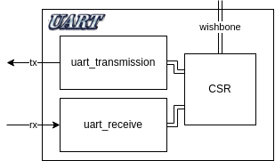
Tranmission
Oraggghhhh !!!!(We should at least be able to make UART with some guts.)
module uart_transmission(
  input wire        rst,
  input wire        clk,
  input wire [31:0] clk_div,
  input wire        tx_start,
  input wire [7:0]  tx_data,
  output reg        tx = 1'b1,
  output reg        clear_req = 1'b0
);

  parameter WAIT        = 4'b0000;
  parameter START_BIT   = 4'b0001;
  parameter SEND_DATA   = 4'b0010;
  parameter STOP_BIT    = 4'b0011;
  parameter CLEAR_REQ   = 4'b0100;

  reg [3:0] state;

  reg [31:0] clk_cnt = 32'h0000_0000;

  reg [2:0] tx_index = 3'b000;

  reg [1:0] detect_posedge_start = 2'b00;

  always @(posedge clk) begin
    if(rst) begin
      tx        <= 1'b1;
      state     <= WAIT;
      clear_req <= 1'b0;
      tx_index  <= 3'b000;
      clk_cnt   <= 32'h0000_0000;
      detect_posedge_start <= 2'b00;
    end else begin
      // for safe
      detect_posedge_start <= {detect_posedge_start[0], tx_start};
      case(state)
        WAIT        : begin
          tx <= 1'b1;
          clear_req <= 1'b0;
          if(detect_posedge_start == 2'b01) begin
            state <= START_BIT;
          end
        end
        START_BIT   : begin
          tx <= 1'b0;
          if(clk_cnt == (clk_div - 1)) begin
            clk_cnt <= 32'h0000_0000;
            state <= SEND_DATA;
          end else begin
            clk_cnt <= clk_cnt + 32'h0000_0001;
          end
        end
        SEND_DATA   : begin
          tx <= tx_data[tx_index];
          if(clk_cnt == (clk_div - 1)) begin
            clk_cnt <= 32'h0000_0000;
            if(tx_index == 3'b111) begin
              state <= STOP_BIT;
            end
            tx_index <= tx_index + 3'b001;
          end else begin
            clk_cnt <= clk_cnt + 32'h0000_0001;
          end
        end
        STOP_BIT    : begin
          tx <= 1'b1;
          if(clk_cnt == (clk_div - 1)) begin
            clk_cnt <= 32'h0000_0000;
            state <= CLEAR_REQ;
          end else begin
            clk_cnt <= clk_cnt + 32'h0000_0001;
          end
        end
        CLEAR_REQ   : begin
          clear_req <= 1'b1;
          state <= WAIT;
        end
        default     : begin
          tx        <= 1'b1;
          state     <= WAIT;
          clear_req <= 1'b0;
          tx_index  <= 3'b000;
          clk_cnt   <= 32'h0000_0000;
          detect_posedge_start <= 2'b00;
        end
      endcase
    end
  end

endmodule
Reception
Oraggghhhh !!!!
module uart_receive (
  input wire        rst,
  input wire        clk,
  input wire [31:0] clk_div,
  input wire        rx,
  input wire        read,
  input wire        irq_en,
  output reg        irq     = 1'b0,
  output reg [7:0]  rx_data = 8'h0
);

  parameter WAIT        = 4'b0000;
  parameter START_BIT   = 4'b0001;
  parameter GET_DATA    = 4'b0010;
  parameter STOP_BIT    = 4'b0011;
  parameter WAIT_READ   = 4'b0100;

  reg [3:0] state;

  reg [31:0] clk_cnt = 32'h0000_0000;

  reg [2:0] rx_index = 3'b000;

  always @(posedge clk) begin
    if(rst) begin
      state     <= WAIT;
      clk_cnt   <= 32'h0000_0000;
      rx_index  <= 3'b000;
      irq       <= 1'b0;
      rx_data   <= 8'h0;
    end else begin
      case(state)
        WAIT      : begin
          irq <= 1'b0;
          if(rx == 1'b0) begin
            state <= START_BIT;
          end
        end
        START_BIT : begin
          // check the middle of wave
          if(clk_cnt == ((clk_div >> 1) - 1)) begin
            clk_cnt <= 32'h0000_0000;
            if(rx == 1'b0) begin
              state <= GET_DATA;
            end
          end else begin
            clk_cnt <= clk_cnt + 32'h0000_0001;
          end
        end
        GET_DATA  : begin
          // get the middle of wave
          if(clk_cnt == (clk_div - 1)) begin
            clk_cnt <= 32'h0000_0000;
            if(rx_index == 3'b111) begin
              state <= STOP_BIT;
            end
            rx_index <= rx_index + 3'b001;
            rx_data[rx_index] <= rx;
          end else begin
            clk_cnt <= clk_cnt + 32'h0000_0001;
          end
        end
        STOP_BIT  : begin
          // check the middle of wave
          if(clk_cnt == (clk_div - 1)) begin
            clk_cnt <= 32'h0000_0000;
            if(rx == 1'b1) begin
              state <= WAIT_READ;
              if(irq_en) begin
                irq <= 1'b1;
              end
            end
          end else begin
            clk_cnt <= clk_cnt + 32'h0000_0001;
          end
        end
        WAIT_READ : begin
          if(read) begin
            irq <= 1'b0;
            state <= WAIT;
          end
        end
        default   : begin
          state     <= WAIT;
          clk_cnt   <= 32'h0000_0000;
          rx_index  <= 3'b000;
          irq       <= 1'b0;
          rx_data   <= 8'h0;
        end
      endcase
    end
  end

endmodule
Top Module
This is not something that can be done in a frenzy, let’s do it carefully.
The most important part is the connection between wishbone and CSR. Please see user_project_wrapper.v. From wb_clk_i to wbs_dat_o are the signal lines of the wishbone used by Caravel. note that the names of the signal lines of RgGen’s wishbone and Caravel’s wishbone are slightly different, but the really important things are as follows.
- Invert
wb_rst_iand input it intoi_rst_n(for negative logic) o_wb_stallis not used- Bit width of
i_wb_adr. - Discriminate
0x3000_00part ofwbs_adr_i. o_wb_erris not used.o_wb_rtyis not used.
In wbs_adr_i, if the upper bits are not 0x3000_00, logic is added to input 0 to cyc and stb of CSR.
Once the wishbone connection is complete, the rest is connecting the CSR data, which is just a matter of connecting them.
Connect the external inputs/outputs io_out and io_in to tx and rx respectively. The pinouts are listed here.
https://caravel-harness.readthedocs.io/en/latest/pinout.html
Since pin 31 is an output and pin 30 is an input, input the values to io_oeb respectively. Since they are negative logic, input 0 if you want to use them as outputs.
The vccd1 and vssd1 are power lines, so I’ll write them down for now.
module uart #(
  parameter BAUD_RATE = 115200
)(
`ifdef USE_POWER_PINS
    inout vccd1,	// User area 1 1.8V supply
    inout vssd1,	// User area 1 digital ground
`endif
  // Wishbone Slave ports (WB MI A)
  input wire    wb_clk_i,
  input wire    wb_rst_i,
  input wire    wbs_stb_i,
  input wire    wbs_cyc_i,
  input wire    wbs_we_i,
  input wire    [3:0] wbs_sel_i,
  input wire    [31:0] wbs_dat_i,
  input wire    [31:0] wbs_adr_i,
  output wire   wbs_ack_o,
  output wire   [31:0] wbs_dat_o,

  // IO ports
  input  [`MPRJ_IO_PADS-1:0] io_in,
  output [`MPRJ_IO_PADS-1:0] io_out,
  output [`MPRJ_IO_PADS-1:0] io_oeb,

  // irq
  output [2:0] user_irq
);

  // UART
  wire  tx;
  wire  rx;

  assign io_oeb[31] =  1'b0;
  assign io_oeb[30] =  1'b1;
  assign io_out[31] = tx;
  assign rx = io_in[30];

  // irq
  wire irq;
  assign user_irq[0] = irq;

  // CSR
  wire [31:0] clk_freq;

  wire [7:0] rx_data;
  wire       irq_en;
  wire       read;

  wire [7:0] tx_data;
  wire tx_clear_req;
  wire tx_start;

  wire i_wb_cyc;
  wire i_wb_stb;

  assign i_wb_cyc = (wbs_adr_i[31:8] == 32'h3000_00) ? wbs_cyc_i : 1'b0;
  assign i_wb_stb = (wbs_adr_i[31:8] == 32'h3000_00) ? wbs_stb_i : 1'b0;

  CSR CSR(
    .i_clk      (wb_clk_i   ),
    .i_rst_n    (~wb_rst_i  ),
    .i_wb_cyc   (i_wb_cyc   ),
    .i_wb_stb   (i_wb_stb   ),
    .o_wb_stall (),
    .i_wb_adr   (wbs_adr_i  ),
    .i_wb_we    (wbs_we_i   ),
    .i_wb_dat   (wbs_dat_i ),
    .i_wb_sel   (wbs_sel_i  ),
    .o_wb_ack   (wbs_ack_o ),
    .o_wb_err   (),
    .o_wb_rty   (),
    .o_wb_dat   (wbs_dat_o  ),
    .o_CLOCK_FREQ_clock_freq            (clk_freq   ),
    .i_RECEIVED_DATA_rx                 (rx_data    ),
    .o_RECEIVED_DATA_rx_read_trigger    (read       ),
    .o_TRANSMISSION_DATA_tx             (tx_data    ),
    .o_INTERRUPT_ENABLE_irq_en          (irq_en     ),
    .i_TRANSMISSION_START_tx_start_clear(tx_clear_req),
    .o_TRANSMISSION_START_tx_start      (tx_start   )
  );

  wire [31:0] clk_div;
  assign clk_div = clk_freq / BAUD_RATE;

  uart_receive      receive(
    .rst        (wb_rst_i   ),
    .clk        (wb_clk_i   ),
    .clk_div    (clk_div    ),
    .rx         (rx         ),
    .rx_data    (rx_data    ),
    .read       (read       ),
    .irq_en     (irq_en     ),
    .irq        (irq        )
  );

  uart_transmission transmission(
    .rst        (wb_rst_i   ),
    .clk        (wb_clk_i   ),
    .clk_div    (clk_div    ),
    .tx         (tx         ),
    .tx_data    (tx_data    ),
    .clear_req  (tx_clear_req),
    .tx_start   (tx_start   )
  );

endmodule
You may be wondering why all the io_in, io_out and io_oeb that are only partially used are pulled into this module. This is because if you only put out tx and rx in uart’s IO and try to connect to io_in[30] and io_out[31] in the user_project_wrapper, you will run into non-trivial LVS errors.
When connecting the user_project_wrapper’s IO to your own module, try to connect the entire signal line, not part of it. The same goes for user_irq.
Next, let’s use OpenLANE to generate GDSII from UART RTL. We are happy to see the layout.
Write configuration file for OpenLANE (UART)
Here we generate GDSII from RTL of UART. First, create a uart directory in the openlane directory and copy and paste the user_proj_example config.
It is not recommended to write a configuration file from scratch in OpenMPW unless you have a complete understanding of integrated circuit design. It is recommended to edit existing configuration files for your own design.
cd caravel_user_project/openlane
mkdir uart
cp user_proj_example/config.json uart/
The config.json may also be config.tcl.
Next, edit the config.json that you have copied and pasted, mostly adding the verilog file path and changing the die size and clock.
The DIE_AREA and PL_TARGET_DENSITY may require some trial and error depending on your design.
{
    "DESIGN_NAME": "uart",
    "DESIGN_IS_CORE": 0,
    "GLB_RT_MAXLAYER": 5,
    "FP_PDN_CHECK_NODES": 0,
    "VERILOG_FILES": [
      "dir::../../verilog/rtl/defines.v",
      "dir::../../verilog/rtl/rggen-verilog-rtl/rggen_rtl_macros.vh",
      "dir::../../verilog/rtl/rggen-verilog-rtl/*.v",
      "dir::../../verilog/rtl/UART/uart.v",
      "dir::../../verilog/rtl/CSR.v",
      "dir::../../verilog/rtl/UART/uart_receive.v",
      "dir::../../verilog/rtl/UART/uart_transmission.v"
    ],

    "CLOCK_PORT": "wb_clk_i",
    "CLOCK_NET": "wb_clk_i",
    "FP_SIZING": "absolute",
    "DIE_AREA": "0 0 400 400",
    "PL_BASIC_PLACEMENT": 0,
    "PL_TARGET_DENSITY": 0.60,
    "ROUTING_CORES": 16,
    "VDD_NETS": ["vccd1"],
    "GND_NETS": ["vssd1"],
    "DIODE_INSERTION_STRATEGY": 4,
    "RUN_CVC": 1,
    "pdk::sky130*": {
        "FP_CORE_UTIL": 45,
        "RT_MAX_LAYER": "met4",
        "scl::sky130_fd_sc_hd": {
            "CLOCK_PERIOD": 100
        },
        "scl::sky130_fd_sc_hdll": {
            "CLOCK_PERIOD": 100
        },
        "scl::sky130_fd_sc_hs": {
            "CLOCK_PERIOD": 100
        },
        "scl::sky130_fd_sc_ls": {
            "CLOCK_PERIOD": 100,
            "SYNTH_MAX_FANOUT": 5
        },
        "scl::sky130_fd_sc_ms": {
            "CLOCK_PERIOD": 100
        }
    },
    "pdk::gf180mcuC": {
        "STD_CELL_LIBRARY": "gf180mcu_fd_sc_mcu7t5v0",
        "CLOCK_PERIOD": 100,
        "FP_CORE_UTIL": 40,
        "RT_MAX_LAYER": "Metal4",
        "SYNTH_MAX_FANOUT": 4,
        "PL_TARGET_DENSITY": 0.45
    }
}
Generate GDSII for UART
After editing the configuration file, run make uart in the repository root. After a short wait, uart.gds is generated in gds/.
cd caravel_user_project
make uart
Here is the uart.gds as seen in klayout. CSRs generated by RgGen are also mixed in here. It is cute.
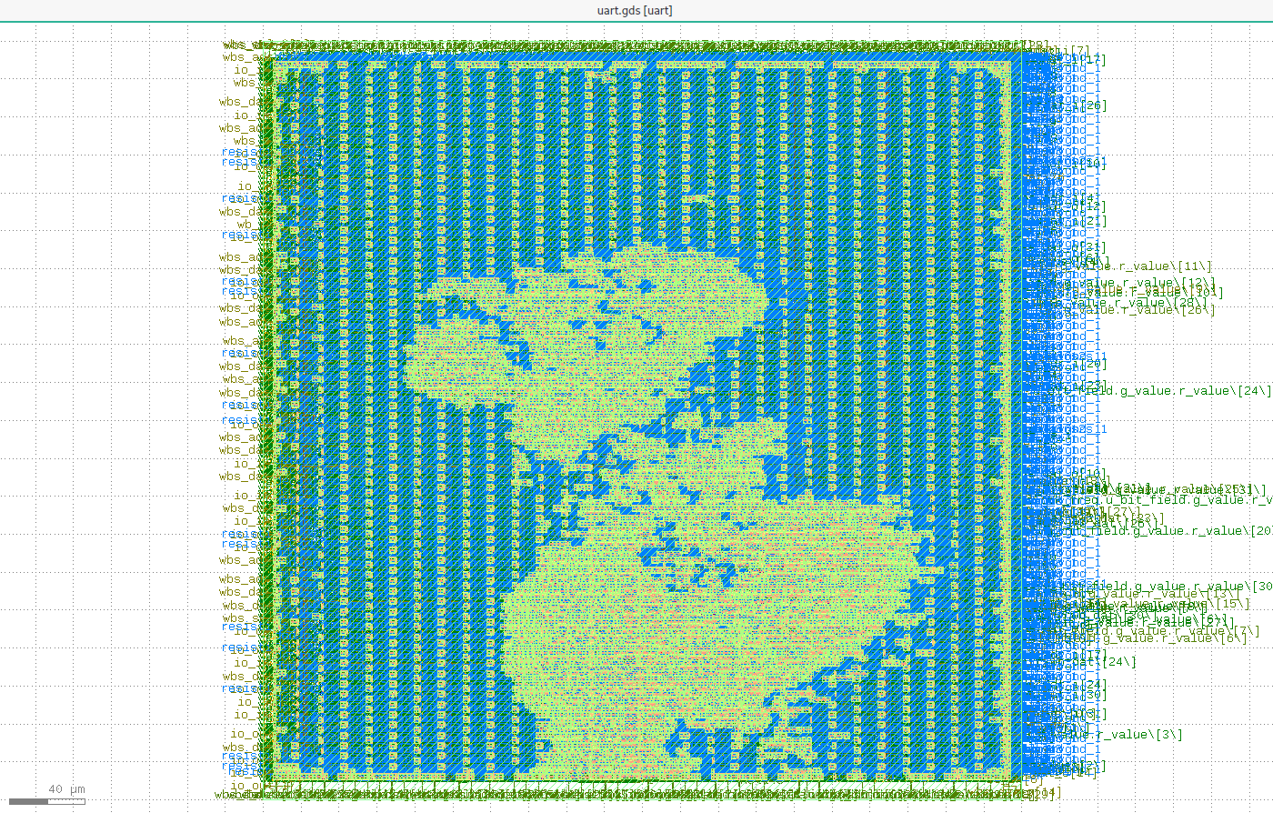
Next, insert this into Caravel’s User Project Area, i.e. user_project_wrapper.v.
Connect to user_project_wrapper
Since user_proj_example is connected by default, we will eliminate it and connect uart.
/*--------------------------------------*/
/* User project is instantiated  here   */
/*--------------------------------------*/

uart uart (
`ifdef USE_POWER_PINS
	.vccd1(vccd1),	// User area 1 1.8V power
	.vssd1(vssd1),	// User area 1 digital ground
`endif
    .wb_clk_i(wb_clk_i),
    .wb_rst_i(wb_rst_i),

    // MGMT SoC Wishbone Slave

    .wbs_stb_i(wbs_stb_i),
    .wbs_cyc_i(wbs_cyc_i),
    .wbs_we_i(wbs_we_i),
    .wbs_sel_i(wbs_sel_i),
    .wbs_dat_i(wbs_dat_i),
    .wbs_adr_i(wbs_adr_i),
    .wbs_ack_o(wbs_ack_o),
    .wbs_dat_o(wbs_dat_o),

    // IO ports
    .io_in  (io_in      ),
    .io_out (io_out     ),
    .io_oeb (io_oeb     ),

    // irq
    .user_irq (user_irq)
);

endmodule	// user_project_wrapper
verilog/rtl/user_project_wrapper.v
Set the initial state of GPIOs with user_defines.v.
As shown above, GPIO No. 31 is used for output and No. 30 for input. Originally, this can be changed dynamically by firmware, but if you edit user_defines.v and set it, No.31 will be output and No.30 will be input from the beginning.
If you don’t have a specific use for a pin, it is easy to set it as an output from the User Project Area.
A part of user_defines.v is shown below.
`define USER_CONFIG_GPIO_27_INIT `GPIO_MODE_USER_STD_OUTPUT
`define USER_CONFIG_GPIO_28_INIT `GPIO_MODE_USER_STD_OUTPUT
`define USER_CONFIG_GPIO_29_INIT `GPIO_MODE_USER_STD_OUTPUT
`define USER_CONFIG_GPIO_30_INIT `GPIO_MODE_USER_STD_INPUT_PULLDOWN
`define USER_CONFIG_GPIO_31_INIT `GPIO_MODE_USER_STD_OUTPUT
`define USER_CONFIG_GPIO_32_INIT `GPIO_MODE_USER_STD_OUTPUT
`define USER_CONFIG_GPIO_33_INIT `GPIO_MODE_USER_STD_OUTPUT
Set the position in macro.cfg
The die size is 3000nmx3000nm, so place it around the center of the die.
uart 1500 1500 N
openlane/user_project_wrapper/macro.cfg
Write OpenLANE configuration file (user_project_wrapper)
Set VERILOG_FILES_BLACKBOX to the path of our Verilog, EXTRA_LEFS and EXTRA_GDS to the paths of files generated under lef/ and gds/. Set the clock period (ns) in CLOCK_PERIOD and the clock signal line in CLOCK_PORT and CLOCK_NET. Then you can increase the number of threads used for wiring by the value of ROUTING_CORES, which is nice to shorten the time.
{
    "DESIGN_NAME": "user_project_wrapper",
    "ROUTING_CORES": 16,
    "VERILOG_FILES": [
      "dir::../../verilog/rtl/defines.v",
      "dir::../../verilog/rtl/user_project_wrapper.v"
    ],
    "CLOCK_PERIOD": 100,
    "CLOCK_PORT": "uart.wb_clk_i",
    "CLOCK_NET": "uart.wb_clk_i",
    "FP_PDN_MACRO_HOOKS": "uart vccd1 vssd1 vccd1 vssd1",
    "MACRO_PLACEMENT_CFG": "dir::macro.cfg",
    "VERILOG_FILES_BLACKBOX": [
      "dir::../../verilog/rtl/defines.v",
      "dir::../../verilog/rtl/UART/uart.v"
    ],
    "EXTRA_LEFS": "dir::../../lef/uart.lef",
    "EXTRA_GDS_FILES": "dir::../../gds/uart.gds",
    "FP_PDN_CHECK_NODES": 0,
    "SYNTH_ELABORATE_ONLY": 1,
openlane/user_project_wrapper/config.json
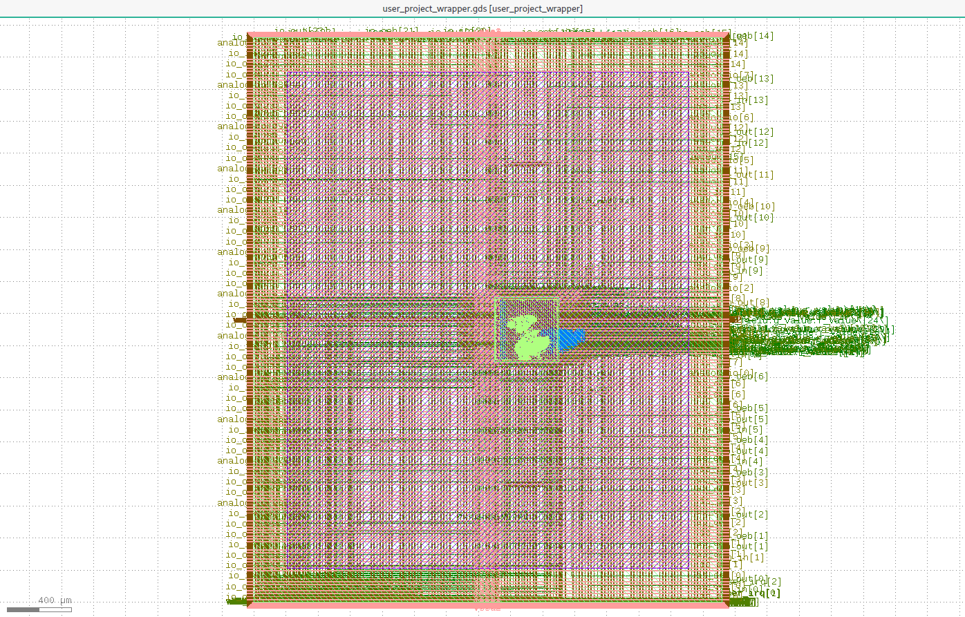
Generate GDSII for user_project_wrapper
Run the following command in the repository root. It’s time to pray. If this succeeds, we are good to go for submission.
make user_project_wrapper
The generated GDSII is shown below. It’s cute.
Create test bench
We’re going to go on a bit longer. Let’s write a testbench to make sure it works correctly.
The testbench is stored under verilog/dv. This is also very painstaking to write from scratch, so copy and edit the existing wb_port.
cd verilog/dv
cp -r wb_port uart_test
Let’s change the file name of the contents for now.
cd uart_test
mv wb_port.c uart_test.c
mv wb_port_tb.v uart_test_tb.v
Next, add the name of the testbench you want to add to the Makefile under verilog/dv/.
PATTERNS = io_ports la_test1 la_test2 wb_port mprj_stimulus uart_test
Then edit all files under verilog/include/.
includes.gl+sdf.caravel_user_project
Add paths to files under verilog/gl
// Caravel user project includes
$USER_PROJECT_VERILOG/gl/user_project_wrapper.v
$USER_PROJECT_VERILOG/gl/uart.v
verilog/includes/includes.gl+sdf.caravel_user_project
includes.gl.caravel_user_project
This also adds the path to the files under verilog/gl, the format is a bit different
# Caravel user project includes
-v $(USER_PROJECT_VERILOG)/gl/user_project_wrapper.v
-v $(USER_PROJECT_VERILOG)/gl/uart.v
verilog/includes/includes.gl.caravel_user_project
includes.rtl.caravel_user_project
Add all the paths to the files you use under verilog/rtl. Use +incdir+ for rggen_rtl_macros.vh since various files are included in it. This file is the cmdfile for icarus verilog, so I stared at the documentation and made it look good, as follows The file is as shown in the following.
# Caravel user project includes
-v $(USER_PROJECT_VERILOG)/rtl/user_project_wrapper.v
+incdir+$(USER_PROJECT_VERILOG)/rtl
+incdir+$(USER_PROJECT_VERILOG)/rtl/rggen-verilog-rtl
-y $(USER_PROJECT_VERILOG)/rtl/rggen-verilog-rtl
-v $(USER_PROJECT_VERILOG)/rtl/CSR.v
-v $(USER_PROJECT_VERILOG)/rtl/UART/uart.v
-v $(USER_PROJECT_VERILOG)/rtl/UART/uart_transmission.v
-v $(USER_PROJECT_VERILOG)/rtl/UART/uart_receive.v
verilog/includes/includes.rtl.caravel_user_project
uart_test_tb.v
Cut out the parts you don’t want from wb_port_tb.v. This is the process of removing what you don’t understand until it becomes something you can understand. This is tedious to explain, so please look at the repository.
verilog/dv/uart_test/uart_test_tb.v
uart_test.c
The program is designed to send A (0x41) using MMIO. Please think of reg_wb_~ and reg_mprj_~ in the beginning as GPIO settings.
#include <defs.h>
#include <stub.c>

#define tx_data (*(volatile uint32_t*)0x30000008)
#define tx_start (*(volatile uint32_t*)0x30000010)


void main()
{
  reg_wb_enable = 1;
  reg_mprj_io_31 = GPIO_MODE_USER_STD_OUTPUT;

  reg_mprj_xfer = 1;
  while (reg_mprj_xfer == 1);

  tx_data = 0x00000041;
  tx_start = 0x000000001;

  while(tx_start != 0x00000000) {}
}
https://github.com/Cra2yPierr0t/caravel_walkthrough_uart/blob/main/verilog/dv/uart_test/uart_test.c
Execute Testbench
Run the following command at the root of the repository to start the test bench. When completed, waveform fals are generated under verilog/dv/uart_test/.
make verify-uart_test-rtl
Then, here is the content of the generated waveform file
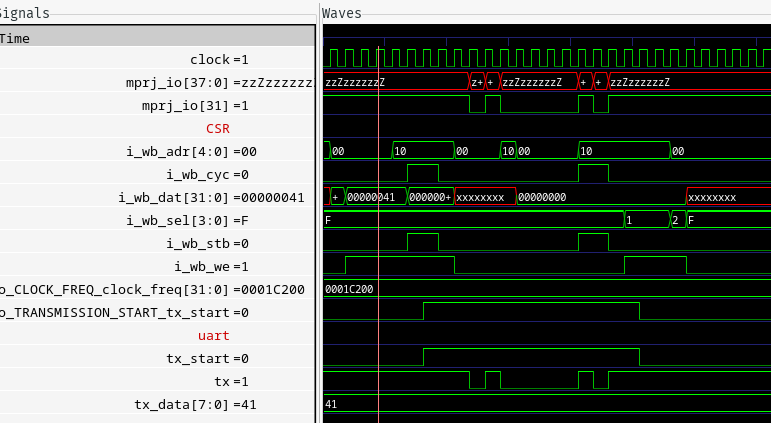
I see 0x41 being sent from mprj_io[31] via UART, and tx_start is also being written and then automatically dropped, wow! It’s seriously working!
Now we’ve even verified that the transmission is working! Yay! I’m not going to do the receiving because I’m too lazy to write a testbench. Well, it should work.
Precheck
Install Docker image for pre-check
make precheck
Execute Precheck
make run-precheck
Pre-check to make sure there are no problems with the design.
submit
Now, we just need to upload the contents of gds/ to a remote repository, register the repository URL at the efabless site, and the submission is complete. That’s easy. Thanks for your time.
Solicitation
If you are interested in OpenMPW, I recommend you join open-source-silicon.dev, the open source semiconductor slack. There are Efabless engineers and other OSS committers here, so if you get stuck, you can ask questions right away. Also, you will see a lot of excitement when the GFMPW-0 and MPW-7 shuttles are being started. By the way, authors are usually in #japan-region. Feel free to talk to me since I’m lonely.
Poem
There is no point in building even an LSI as a personal hobby. Because FPGA is enough to verify the HDL at hand. But because we have FPGA, because we can verify with FPGA, I think it’s okay to go one step further and make it to LSI. Because Google has prepared OpenMPW and said that even you can make an LSI. And it’s free. I am also writing this article to lower the hurdle. If you can do it, why don’t you give it a try?