Introduction to OpenMPW
Questions, suggested revisions, or other communications can be sent to @Cra2yPierr0t
It’s been a while since I read the introductory article I wrote before, but the writing was messy, the content was old, and it was done like the end of the world, so I’m writing this in preparation for 90nm.
Want to make your own LSI? Let’s make it. Skywater opened its PDK to the public, and OpenLANE, an OSS GDSII compiler, was born. And Efabless, funded by Google, has started the Open MPW Shuttle Program, a program that lets you build LSIs for free. Now is your chance to create your own LSI. Build the chip you want to build, on Google’s dime!
OpenMPW Overview
OpenMPW (Open Multi Project Wafer) is a shuttle program created by Google’s investment in Efabless, and its home page includes the following statement.
The shuttle provides opportunities for designers to experiment and push the state-of-the-art without having to reconcile the risk associated with the cost of fabrication. The shuttle program is open to anyone, provided that their project is fully open source and meets the other program requirements. Costs for fabrication, packaging, evaluation boards and shipping are covered by Google for this program.
Source: https://efabless.com/open_shuttle_program
So it’s a program where you can make your own semiconductors completely free of charge as long as you makes your design open source. This is hot, you have to join, Google is the best! I will follow you for the rest of my life.
That said, not all submitted designs will be made into LSI, and several conditions exist.
- 40 projects will be randomly selected from the submissions
- Use of the Skywater PDK
- Making your design open source
- The layout must be reproducible from the repository
- Various licenses
- Use of Caravel (see below)
- Must pass pre-checking tools
I know you want to make your own HDL into LSI right now, but there is a bit much that needs to be done, so let’s do it little by little.
Next, we will go into an overview of each tool, which you may skip if you already know and have installed it.
OpenLANE Overview
OpenLANE is an OSS RTL-to-GDSII compiler, which is made by combining about 20 OSS.
When this GDSII is sent to a fab, it will build an LSI.
OpenLANE provides a Docker container, and it is recommended to install OpenLANE using Docker. It is possible to install OpenLANE without using Docker container, but you should stay away from it because it says “It is more complex” or something like that.
environment building
Build an environment to install OpenLANE; supports Linux/M1 Mac/Intel Mac/Win.
Minimum requirements are here
- GNU Make
- Python 3.6+ with pip and virtualenv
- Git 2.22+ with pip and virtualenv
- Docker 19.03.12+.
The following commands are targeted at Ubuntu and Archlinux, but can be used on any OS with pip, virtualenv and docker.
Installing pip and virtualenv
Ubuntu
sudo apt install python3-venv python3-pip
Archlinux
sudo pacman -S python-virtualenv python-pip
Installing docker
Ubuntu
sudo apt install docker.io
Archlinux
sudo pacman -S docker
Add yourself to the docker group. This is very bad for security. I tried using podman and other ways to get around this, but in the end it was impossible in my environment, so I gave up. If you can work around this, please let me know.
Ubuntu, Archlinux
sudo usermod -a -G docker $(whoami)
Restart once.
Start the Docker daemon
Ubuntu, Archlinux
systemctl start docker
Installing OpenLANE
Next, install OpenLANE, but install caravel first because it is more convenient to install via caravel, which is described later.
Download caravel first. The <tag> should be the latest one from the following page. At the time of writing, it is mpw-8c for shuttles using Skywater’s 130nm and gfmpw-0d for GlobalFoundries’ 180nm.
https://github.com/efabless/caravel_user_project/tags
git clone -branch <tag> https://github.com/efabless/caravel_user_project.git
Then create a dependencies directory, a directory to install OpenLANE and PDK, and set environment variables.
cd caravel_user_project
mkdir dependencies
export OPENLANE_ROOT=$(pwd)/dependencies/openlane_src
export PDK_ROOT=$(pwd)/dependencies/pdks
Next, set the type of PDK to be installed; a PDK contains blueprints for OR circuits, AND circuits, FF, etc.
The <pdk> field specifies the type of PDK you want to install, such as sky130A, sky130B, gf180mcuC, etc. Select the type according to the process to be used in the shuttle.
export PDK=<pdk>
Start installation with make setup.
make setup
The environment variables OPENLANE_ROOT and PDK_ROOT are important; if they are not set, neither OpenLANE nor Caravel will work.
Checking the operation of OpenLANE
You can enter the OpenLANE directory and use make to check the operation.
cd $OPENLANE_ROOT
make test
If “Basic test passed” is displayed, the installation has been completed without any problems.

If you want to build a design under design/ that is already prepared, you can make mount and then use . /flow.tcl -design <directory name>.
The following is a command to build APU as a trial.
cd $OPENLANE_ROOT
make mount
./flow.tcl -design APU
The GDSII generated when the design was built directly using OpenLANE is
OpenLANE/designs/APU/runs/run_<date>/results/final/gds and the layout can be viewed using klayout.
klayout APU.gds

This image hides the decap cells to give a sense of the circuit being generated and is slightly different from what is actually seen.
Configuration of OpenLANE
When using OpenLANE, it is necessary to write a configuration file for OpenLANE according to the design as well as writing HDL.
Let’s look at the configuration file for the default design. The default designs are located under OpenLANE/designs/ which includes usb, picorv32a, etc. config.tcl in those directories is the OpenLANE configuration file.
The configuration file can be set either in the tcl file config.tcl or in the json file config.json.
A basic description of how to write a configuration file can be found here, but will be explained later.
https://openlane.readthedocs.io/en/latest/usage/hardening_macros.html
A list of available variables can be found here, and the essential variables will be explained later.
https://openlane.readthedocs.io/en/latest/reference/configuration.html
Caravel Overview
Caravel, which has been mentioned many times before, is an OpenMPW semiconductor design template. Caravel is a template for OpenMPW semiconductor design, which allows you to build, precheck, and testbench your design with a single template.
Caravel is divided into Management Area and User Project Area. The Management Area is an area that cannot be changed and consists of a lightweight RISC-V core and various IOs. The User Project Area is an area that can be freely modified, where developers place their designs.
The size of the Management Area is 2.920um x 3.520um, which is roughly 10mm.
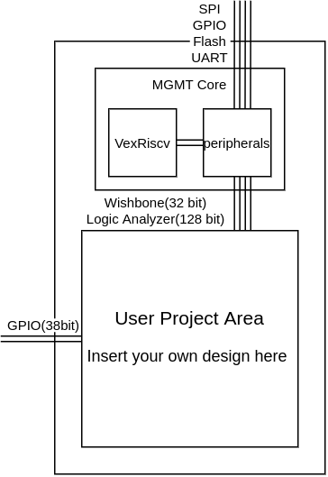
There are 38 GPIO lines extending out from the User Project Area, from which you can directly access your design. The Management Area is connected to the RISC-V core via a 32-bit wishbone interface and 128-bit Logic Analyzer lines, allowing programs running on the RISC-V core to access the RISC-V core via MMIO.
Installing Caravel
If you have already installed Caravel by installing OpenLANE above, you do not need to do this step. It is better not to do it.
However, if you want to delete OpenLANE, pdk, Caravel, and everything else and install the OSS you need with OpenMPW again, this is a quick way to do it.
Download caravel. The <tag> should be the latest one from the following page. At the time of writing, it is mpw-8c for shuttles using Skywater’s 130nm and gfmpw-0d for GlobalFoundries’ 180nm.
https://github.com/efabless/caravel_user_project/tags
git clone -branch <tag> https://github.com/efabless/caravel_user_project.git
Create a dependencies directory, a directory to install OpenLANE and PDK, and set environment variables.
cd caravel_user_project
mkdir dependencies
export OPENLANE_ROOT=$(pwd)/dependencies/openlane_src
export PDK_ROOT=$(pwd)/dependencies/pdks
Next, set the type of PDK to be installed; a PDK contains blueprints for OR circuits, AND circuits, FF, etc.
The <pdk> field specifies the type of PDK you want to install, such as sky130A, sky130B, gf180mcuC, etc. Select the type according to the process to be used in the shuttle.
export PDK=<pdk>
Start installation.
make setup
Checking that Caravel is working
You can go under caravel_user_project and build the design provided as an example using make.
make user_proj_example
GDSII files are generated under gds/.
Caravel File Structure
To use Caravel, it is sufficient to know how to use the following four directories.
gds/: GDSII files are generated here.openlane/: OpenLANE configuration files are placed here.verilog/dv/: put simulation and testbench files here.verilog/rtl/: put verilog files of your own design here
A description of all Caravel directories can be found here.
https://caravel-harness.readthedocs.io/en/latest/getting-started.html#required-directory-structure
In Caravel, the design build is divided into two stages. The first stage is the build of your Verilog, and the second stage is the build of the wrapper. In OpenMPW, the wrapper is submitted.
The wrapper here is a design that contains one or more of your designs and is named user_project_wrapper.
The built user_project_wrapper usually looks like the image below, with the design inserted into the wrapper.

This image also hides the decap cells to give the feeling that a circuit is being generated.
The developer edits two OpenLANE configuration files, one for own design and one for user_project_wrapper. The latter one is only slightly edited, so don’t worry about it.
Since user_project_wrapper contains user_proj_example immediately after installation of Caravel, building user_proj_wrapper after building user_project_wrapper will result in GDSII will be generated as shown in the image above.
make user_proj_example
make user_project_wrapper

klayout gds/user_project_wrapper.gds
Caravel Documentation
The Caravel documentation can be found here and will be explained in detail later.
https://caravel-harness.readthedocs.io/en/latest/index.html#
Make your design LSI with OpenMPW!
From here, I will explain how to build your own design in earnest and submit it to OpenMPW. Note that we will not explain how to write Verilog, so please prepare your own design.
Here is what you need. The above three have already been done in the previous chapter.
- Caravel_user_project : Add your own design to the User Project Area.
- Skywater PDK : Process Design Kit, like material information.
- OpenLANE : Compiler to convert RTL to GDSII (not necessary if you have Synopsys or something)
- Your own design
- Time, mental energy : lots of it.
1. prepare the design you want to bake
First, let’s prepare your design. We will use Ethernet MAC as an example.
https://github.com/Cra2yPierr0t/Vthernet-SoC/tree/main/verilog/rtl/Vthernet_MAC
I made it for you.
2. create an interface for Caravel in your own design.
If you connect your design to Caravel’s MGMT Core, you will be able to set registers and send and receive data. Also, if you connect your design to an external pin, you can directly send and receive data to and from the outside.
This section describes what you need to do to make your design compatible with Caravel.
There are two ways to connect to the Management Core: Wishbone and Logic Analyzer. There is one way to connect to the outside world, named mprj_io.
To summarize.
| Signal Name | Bus Width | Direction |
|---|---|---|
| Wishbone | 32bit | user_design <-> Management Core |
| Logic Analyzer | 128bit | user_design <-> Management Core |
| mprj_io | 38bit | user_design <-> Outside |
Difference between Wishbone and Logic Analyzer
I mentioned that there are two ways to communicate between your design and MGMT Core: Wishbone (32 bits wide) and Logic Analyzer (128 bits wide). So, here is a quick overview of the two.
Wishbone is a communication protocol, a friend of AXI4 and AMBA, which allows read and write operations by manipulating 10 types of signal lines according to the protocol. In Caravel, addresses from 0x30000000 to 0x80000000-1 are reserved for the Wishbone and can be used freely within this range.
Next is Logic Analyzer, which is just a signal line name. The bus width is 128 bits, four times wider than the Wishbone, and there are no separate data lines or address lines, only three types of signal lines. From MGMT Core, 128 bits are divided into four parts, 0x250000000, 0x250000004, 0x250000008, and 0x25000000c, which are visible as four registers.
Logic Analyzer is easier to implement in HDL, but only four addresses can be allocated. Wishbone, on the other hand, is a bit more complicated than Logic Analyzer in terms of simplicity, but it can handle a wider range of addresses. Well, which one is better suited for which application, so this section describes how to use both.
Creating a Wishbone interface
This section explains how to create a mechanism to read data from and write data to registers in Wishbone. By creating this interface, the RISC-V processor will be able to send and receive data to and from your design via MMIO.
The signal lines of Wishbone are as follows.
| Signal Name | Direction | Function |
|---|---|---|
wb_clk_i |
MGMT Core -> user_design | Clock input from the master. The value is read at the timing of this rising edge. |
wb_rst_i |
MGMT Core -> user_design | Reset signal. |
wbs_stb_i |
MGMT Core -> user_design | Strobe input. Indicates that a slave is selected. |
wbs_cyc_i |
MGMT Core -> user_design | Cycle Input. Indicates that a valid bus cycle is in progress. |
wbs_we_i |
MGMT Core -> user_design | Write enable input. 1 for Write, 0 for Read. |
wbs_sel_i[3:0] |
MGMT Core -> user_design | Selector input. Indicates which bytes of wbs_dat_i[31:0] are valid. 8-bit granularity. |
wbs_dat_i[31:0] |
MGMT Core -> user_design | Data input. |
wbs_adr_i[31:0] |
MGMT Core -> user_design | Address input. |
wbs_ack_o |
MGMT Core <- user_design | Acknowledge output. 1 indicates the end of a normal bus cycle. |
wbs_dat_o[31:0] |
MGMT Core <- user_design | Data output. |
There are 10 signal lines, which may scare those who have not dealt with communication protocols such as AXI4 and AMBA very much, but it is very simple to handle. First, the waveforms of READ and WRITE are shown below. This was borrowed from the Wishbone specification.
Waveform of READ
 READ is an operation that sends data to the MGMT Core (MGMT Core is the Master) and takes two cycles to complete.
Waveform of WRITE
 WRITE is an operation to receive data from the MGMT Core and is completed in two cycles as well.
The protocol is explained below.
WRITE is an operation to receive data from the MGMT Core and is completed in two cycles as well.
The protocol is explained below.
First of all, there are three signal lines, adr_o, dat_i, and dat_o, which you should know as a prerequisite. Each adr_o is an address line, dat_i is data to MGMT Core (for READ), and dat_o is data from MGMT Core (for WRITE).
The first two to look at in the first cycle are stb_o and cyc_o. If these two are present, it means that you have been selected and communication has been initiated. Next, if we_o is standing, it means that WRITE is performed in that cycle, and if not, READ is performed. If WRITE, adr_o and dat_o are valid values, and the value of dat_o should be placed at the destination specified by adr_o. If READ, adr_o is the address of the desired data.
The first thing to look at in the second cycle is dat_i and ack_i. The dat_i is used only in the case of READ, and the data specified by adr_o is input here. The ack_i is used for both READ and WRITE, and indicates the completion of communication by standing up in this cycle.
I’ve explained it in detail, but you can see it by looking at the waveforms. Also, wbs_sel_i is byte-enabled.
The specs say all sorts of things about pipelined transactions and such, but Caravel probably doesn’t do consecutive transactions, and the transactions are supposed to be spaced apart from each other. At least that was the case in the simulation.
The following is a Wishbone interface created by the author for reference in implementation. (License free!)
module wb_interface #(
    parameter TEST_CSR0 = 32'h3000_0000,
    parameter TEST_CSR1 = 32'h3000_0004,
    parameter TEST_CSR2 = 32'h3000_0008
)(
    // wishbone signals
    input   wire        wb_clk_i,
    input   wire        wb_rst_i,
    input   wire        wbs_stb_i,
    input   wire        wbs_cyc_i,
    input   wire        wbs_we_i,
    input   wire [3:0]  wbs_sel_i,
    input   wire [31:0] wbs_dat_i,
    input   wire [31:0] wbs_adr_i,
    output  reg         wbs_ack_o,
    output  reg  [31:0] wbs_dat_o,
    // CSRs
    output  reg  [31:0] test_csr0,
    output  reg  [31:0] test_csr1,
    output  reg  [31:0] test_csr2
);

    localparam WB_IDLE  = 2'b00;
    localparam WB_READ  = 2'b01;
    localparam WB_WRITE = 2'b10;

    reg [1:0] wb_state;

    always @(posedge wb_clk_i) begin
        if(wb_rst_i) begin
            wb_state    <= WB_IDLE;
            wbs_ack_o   <= 1'b0;
        end else begin
            case(wb_state)
                WB_IDLE : begin
                    wbs_ack_o   <= 1'b0;
                    if(wbs_stb_i && wbs_cyc_i) begin
                        if(wbs_we_i) begin
                            wb_state <= WB_WRITE;
                        end else begin
                            wb_state <= WB_READ;
                        end
                    end
                end
                WB_READ : begin
                    wb_state    <= WB_IDLE;
                    wbs_ack_o   <= 1'b1;
                    case(wbs_adr_i)
                        TEST_CSR0 : begin
                            wbs_dat_o[7:0]   <= wbs_sel_i[0] ? test_csr0[7:0] : 8'h00;
                            wbs_dat_o[15:8]  <= wbs_sel_i[1] ? test_csr0[15:0] : 8'h00;
                            wbs_dat_o[23:16] <= wbs_sel_i[2] ? test_csr0[23:16] : 8'h00;
                            wbs_dat_o[31:24] <= wbs_sel_i[3] ? test_csr0[31:24] : 8'h00;
                        end
                        TEST_CSR1 : begin
                            wbs_dat_o[7:0]   <= wbs_sel_i[0] ? test_csr1[7:0] : 8'h00;
                            wbs_dat_o[15:8]  <= wbs_sel_i[1] ? test_csr1[15:0] : 8'h00;
                            wbs_dat_o[23:16] <= wbs_sel_i[2] ? test_csr1[23:16] : 8'h00;
                            wbs_dat_o[31:24] <= wbs_sel_i[3] ? test_csr1[31:24] : 8'h00;
                        end
                        TEST_CSR2 : begin
                            wbs_dat_o[7:0]   <= wbs_sel_i[0] ? test_csr2[7:0] : 8'h00;
                            wbs_dat_o[15:8]  <= wbs_sel_i[1] ? test_csr2[15:0] : 8'h00;
                            wbs_dat_o[23:16] <= wbs_sel_i[2] ? test_csr2[23:16] : 8'h00;
                            wbs_dat_o[31:24] <= wbs_sel_i[3] ? test_csr2[31:24] : 8'h00;
                        end
                        default   : begin
                            wbs_dat_o <= 32'h0000_0000;
                        end
                    endcase
                end
                WB_WRITE : begin
                    wb_state    <= WB_IDLE;
                    wbs_ack_o   <= 1'b1;
                    case(wbs_adr_i)
                        TEST_CSR0 : begin
                            test_csr0[7:0]   <= wbs_sel_i[0] ? wbs_dat_i[7:0] : 8'h00;
                            test_csr0[15:8]  <= wbs_sel_i[1] ? wbs_dat_i[15:8] : 8'h00;
                            test_csr0[23:16] <= wbs_sel_i[2] ? wbs_dat_i[23:16] : 8'h00;
                            test_csr0[31:24] <= wbs_sel_i[3] ? wbs_dat_i[31:24] : 8'h00;
                        end
                        TEST_CSR1 : begin
                            test_csr1[7:0]   <= wbs_sel_i[0] ? wbs_dat_i[7:0] : 8'h00;
                            test_csr1[15:8]  <= wbs_sel_i[1] ? wbs_dat_i[15:8] : 8'h00;
                            test_csr1[23:16] <= wbs_sel_i[2] ? wbs_dat_i[23:16] : 8'h00;
                            test_csr1[31:24] <= wbs_sel_i[3] ? wbs_dat_i[31:24] : 8'h00;
                        end
                        TEST_CSR2 : begin
                            test_csr2[7:0]   <= wbs_sel_i[0] ? wbs_dat_i[7:0] : 8'h00;
                            test_csr2[15:8]  <= wbs_sel_i[1] ? wbs_dat_i[15:8] : 8'h00;
                            test_csr2[23:16] <= wbs_sel_i[2] ? wbs_dat_i[23:16] : 8'h00;
                            test_csr2[31:24] <= wbs_sel_i[3] ? wbs_dat_i[31:24] : 8'h00;
                        end
                    endcase
                end
            endcase
        end
    end

endmodule
It will probably work.
Handling Logic Analyzer
Logic Analyzer can receive and send 128-bit data. The following three types of signal lines are used in Logic Analyzer.
| Signal Name | Direction | Function |
|---|---|---|
la_data_in |
MGMT Core -> user_design | Data input |
la_data_out |
MGMT Core <- user_diesgn | Data output |
la_oenb |
MGMT Core -> user_deisgn | data output enable bar |
la_data_in is the data input, where data from the Logic Analyzer comes through. The la_data_out is the data output, and data to the Logic Analyzer is sent here. Of note is la_oenb. This is a signal that indicates whether la_data_in or la_data_out is enabled, and is input from the MGMT Core. In other words, the MGMT Core determines which line of the 128-bit Logic Analyzer is for input and which line is for output through the MMIO.
Since la_data_oenb is a data output enable bar, the output (la_data_out) is enabled when 0 and the input (la_data_in) when 1. Easy to remember as 0utput and 1nput.
The following is an example of using Logic Analyzer for reference in implementation.
assign la_data_out[31:0] = test_signals;
assign w_super_data = (&la_oenb[63:32]) ? la_data_in[63:32] : 32'h0000_0000;
It is rather easy to handle. Incidentally, the & in the second line is a reduction operator.
Handling mprj_io
By using mprj_io, you can directly exchange 38-bit signals between your design and the outside world. The following three types of signal lines are handled by mprj_io.
| Signal Name | Direction | Function |
|---|---|---|
io_in |
MGMT Core -> user_design | Data input |
io_out |
MGMT Core <- user_diesgn | Data output |
io_oenb |
MGMT Core <- user_deisgn | data output enable bar |
It is very similar to Logic Analyzer, but note the io_oenb. The direction of the signal is different from Logic Analyzer, and it is an output from your design. Therefore, you can decide which line to use for output and which line to use for input in your design.
Since io_oenb is a data output enable bar, output (io_out) is enabled when it is 0 and input (io_in) when it is 1. It is easy to remember them as 0utput and 1nput.
You need to configure various settings on the firmware side, but in your design, you only need to manipulate the value of io_oenb.
The following is an example of using mprj_io, and I hope it will be helpful for your implementation.
assign io_enb[31:0]  = 32'hffff_ffff;
assign io_enb[32]    = 1'b1;
assign io_enb[34:33] = 2'b00;
assign data_in = io_in[31:0];
assign hard_reset = io_in[32];
assign io_out[34:33] = led[1:0];
And so on. It is probably appropriate to use assign or always for input to io_out.
How to handle interrupts
Caravel can apply interrupts to MGMT Core from its own design.
For interrupts, a 3-bit wide signal line of user_irq[2:0] is used. An interrupt is generated when any one of these 3 bits stands. When an interrupt occurs, the program counter of MGMT Core is set to 0x00000000.
Therefore, the interrupt handler should be placed at 0x00000000 in memory.
You need to set the CSR of MGMT Core in firmware to enable interrupts, but in your own design, you only need to set user_irq when you want to interrupt.
This video is very helpful; Interrupt!
https://www.youtube.com/watch?v=pPgnVBguNW8
3. convert your own design to GDSII
Once your design is ready for Caravel, convert it to GDSII. This operation is called “Hardening”. Also, the hardened design is called a macro.
Writing a configuration file
First, make sure that the Verilog file of your design is under verilog/rtl. If not, bring it.
Next, create a directory under openlane to store the configuration files for OpenLANE. The name of this directory should be the same as the name of the top level module.
mkdir openlane/<user design top module>
The configuration file is placed in the directory created above, but it is very hard to write from scratch. Therefore, copy and edit the configuration file for user_proj_example, which is provided as an example.
Copying the configuration file
cd openlane/<user design top module>
cp ../user_proj_example/config.tcl .
From here, I will explain the parts of the config.tcl that you copied and should edit.
First of all, tcl itself is sufficient for OpenLANE if you remember the following syntax.
set ::env(VAR_NAME) value
This sets the value value to a variable named VAR_NAME. Hereafter, “variable” refers to this VAR_NAME and similar ones.
The first two variables to change in config.tcl are DESIGN_NAME and VERILOG_FILES.
The DESIGN_NAME is literally the name of the design, and should be the same name as the top-level module. VERILOG_FILES is the path to the Verilog file to be synthesized.
An example of how to write it is shown below. Multiple Verilog files can be specified in VERILOG_FILES.
set ::env(DESIGN_NAME) user_design_top_module

set ::env(VERILOG_FILES) "\
    $::env(CARAVEL_ROOT)/verilog/rtl/defines.v \
    $script_dir/../../verilog/rtl/user_design_top_module.v \
    $script_dir/../../verilog/rtl/user_design_sub_module.v"
There is a mysterious variable $script_dir, which is the location of the config.tcl you are currently reading. It is very likely that $script_dir will disappear and be changed to $DESIGN_DIR in the future.
The next three variables to change are CLOCK_PORT, CLOCK_NET, and CLOCK_PERIOD, which are related to the clock. The CLOCK_PORT specifies the port used for the clock input of the design, and the CLOCK_NET I honestly don’t know. The documentation says that CLOCK_PORT is for STA and CLOCK_NET is for CTS, but I think it’s probably OK to set the same value.
Set the clock period in nanoseconds in CLOCK_PERIOD. If you set 10, the clock period is 100 MHz.
An example is shown below. I would like someone to tell me about CLOCK_NET.
set ::env(CLOCK_PORT) "wb_clk_i"
set ::env(CLOCK_NET) $::env(CLOCK_PORT)
set ::env(CLOCK_PERIOD) "10"
The next thing to change is DIE_AREA. This sets the size of the macro in micrometers. The order of the settings is x0 y0 x1 y1. If you set "0 0 200 100", the size will be a rectangle of 200umx100um. The coordinates are the same as in the first quadrant.
You can use any combination of coordinates at first, and seek the best combination with PL_TARGET_DENSITY described later.
An example is shown below.
set ::env(DIE_AREA) "0 0 900 600"
The next change is in FP_PIN_ORDER_CFG, which sets the direction from which pins will be placed in the macro. However, since OpenLANE will do it by itself without setting it, please remove it by commenting it out or deleting the whole line.
The commented out example is shown below.
#set ::env(FP_PIN_ORDER_CFG) $script_dir/pin_order.cfg
If you need it, please set it by yourself.
The last thing to change is PL_TARGET_DENSITY. This determines how densely the area of the DIE_AREA setting will be placed. The value can be a real number between 0 and 1. If you set an extreme value between 0 and 1, OpenLANE will tell you the best value, so you can use that as a reference.
An example is shown below.
set ::env(PL_TARGET_DENSITY) 0.2
The following table summarizes the variables that should be changed.
| Variable name | Function | Remarks |
|---|---|---|
DESIGN_NAME |
specifies a top-level module | |
VERILOG_FILES |
Specify the Verilog files | |
CLOCK_PORT |
Specify the clock port | |
CLOCK_NET |
Mystery | Mystery |
CLOCK_PERIOD |
Specify the clock period | in nanoseconds |
DIE_AREA |
Specify the size of the macro | in micrometersx0 y0 x1 y1 |
FP_PIN_ORDER_CFG |
Specify the direction of the pin | delete |
PL_TARGET_DENSITY |
Specify the placement density | 0~1 |
Generate GDSII
Once the configuration file is complete, the next step is to generate GDSII. The build is started by running make <design_name> under caravel_user_project/.
make <user design top module>
The generated GDSII exists in openlane/<user design top module>/runs/run_<date>/results/final/gds and the layout can be viewed using klayout.
klayout <user design top module>.gds
Cute.
4. add your own design to user_project_wrapper
Simply put your own module in verilog/rtl/user_project_wrapper.v instead of user_proj_example. Note that it is not recommended to set up logic such as AND and NOT in user_project_wrapper, as it may cause unexpected errors.
PS: Edit user_defines.v
Edit verilog/rtl/user_defines.v to set IO state. Change all GPIO_MODE_INVALID to GPIO_MODE_USER_STD_OUTPUT, GPIO_MODE_USER_STD_INPUT_PULLDOWN, etc. depending on your design.
5. check the operation by simulation
Once you have connected your design to Caravel, the next step is to check its operation in simulation.
In order to run the simulation, it is necessary to write a few settings and a test bench for the firmware to be run on the MGMT Core and what signals to input to io_in, etc. I will explain in turn.
Installing the simulation environment
First, install the environment for simulation with this command.
make simenv
Specify the file to use
Just as you set the path to the Verilog files for your design in OpenLANE to config.tcl, in simulation, you need to tell the simulation environment which files to use.
There are three configuration files that need to be edited.
verilog/includes/includes.gl+sdf.caravel_user_projectverilog/includes/includes.gl.caravel_user_projectverilog/includes/includes.rtl.caravel_user_project
First, regarding includes.rtl.caravel_user_project, add the path to the Verilog files you need for your design, including the user_project_wrapper.
An example is given below.
-v $(USER_PROJECT_VERILOG)/rtl/user_project_wrapper.v
-v $(USER_PROJECT_VERILOG)/rtl/user_design_top_module.v
-v $(USER_PROJECT_VERILOG)/rtl/user_design_sub_module.v
Next, for includes.gl.caravel_user_project, add the path to the Verilog files generated in verilog/gl/. The files in verilog/gl/ are automatically generated and are a collection of multiple Verilog files.
An example is shown below.
-v $(USER_PROJECT_VERILOG)/gl/user_project_wrapper.v
-v $(USER_PROJECT_VERILOG)/gl/user_design_top_module.v
Finally, for includes.gl+sdf.caravel_user_project, add the path to the file under verilog/gl/ as well as includes.gl.caravel_user_project.
An example is shown below.
$USER_PROJECT_VERILOG/gl/user_project_wrapper.v
$USER_PROJECT_VERILOG/gl/user_design_top_module.v
The setup is now complete.
Writing the firmware
The firmware can be written in C. Caravel will pull a Docker container containing the RISCV toolchain, so you can run the make command to compile the firmware or whatever.
First, create a directory for the simulation in verilog/dv.
mkdir verilog/dv/<sim_name>
Store the firmware and test bench in this directory.
The name of the firmware should be <sim_name>.c. Hereafter, we will explain how to write the firmware.
First, include two files.
#include <defs.h>
#include <stub.c>
Various global variables and constants are defined in this defs.h.
https://github.com/efabless/caravel/blob/main/verilog/dv/caravel/defs.h
The rest of the program is written in the main function, but you may define functions and split files as in ordinary C language.
The configuration part of CSR should be written as follows.
reg_mprj_io_0   = GPIO_MODE_USER_STD_INPUT_PULLDOWN;
reg_mprj_io_1   = GPIO_MODE_USER_STD_INPUT_PULLDOWN;
reg_mprj_io_2   = GPIO_MODE_USER_STD_INPUT_PULLDOWN;
reg_mprj_io_3   = GPIO_MODE_USER_STD_INPUT_PULLDOWN;
reg_mprj_io_4   = GPIO_MODE_USER_STD_INPUT_PULLDOWN;
reg_mprj_io_5   = GPIO_MODE_USER_STD_INPUT_PULLDOWN;
reg_mprj_io_6   = GPIO_MODE_USER_STD_INPUT_PULLDOWN;
reg_mprj_io_7   = GPIO_MODE_USER_STD_INPUT_PULLDOWN;
reg_mprj_io_33  = GPIO_MODE_USER_STD_OUTPUT;
reg_mprj_io_34  = GPIO_MODE_USER_STD_OUTPUT;

reg_mprj_xfer = 1;
while (reg_mprj_xfer == 1);
In the above example, mprj_io[7:0] is set as input and mprj_io[34:33] as output.
The part of reg_mprj_xfer, while after that is the part where the settings are applied, and when the settings are applied, it exits from the while statement. The mechanism here is unknown.
GPIO_MODE_USER_STD_INPUT_PULLDOWN is a constant that sets mprj_io to the input of pulldown, and GPIO_MODE_USER_STD_OUTPUT to the output.
Other constants such as GPIO_MODE_MGMT_STD_OUTPUT and GPIO_MODE_MGMT_STD_INPUT_PULLDOWN can be set, in which case signals can be sent and received between the MGMT Core and GPIO.
Basically, you can write the setting before while(reg_mprj_xfer == 1) and the processing after that.
Write a test bench
Since it is very troublesome to write a testbench from scratch, an existing testbench is copied and pasted and used. As an example, we use io_ports/io_ports_tb.v as a starting point.
Copy Test Bench
cp ./dv/io_ports/io_ports_tb.v ./dv/<sim_name>/<sim_name>_tb.v
In the following, we will make the necessary configuration changes.
First, change the name of the test bench.
module <sim_name>_tb;
Below that is a spooky area surrounded by ifdef ENABLE_SDF, but there is no need to edit this area.
Next, change the target and name of the waveform file.
initial begin
    $dumpfile("<sim_name>.vcd");
    $dumpvars(0, <sim_name>_tb);
    ...
Next, rename the file to be loaded into spiflash at the bottom of the file.
spiflash #(
    .FILENAME("<sim_name>.hex")
) spiflash (
...
That’s all for the setup. After this is done, write your own signals in the initial statement starting at line 162.
https://github.com/efabless/caravel_user_project/blob/main/verilog/dv/io_ports/io_ports_tb.v#L162
An example is given below. Don’t worry about the ifdef GL in the original file. Just remember $finish;.
initial begin
    mprj_io[7:0] <= 8'h55;
    # 100
    mprj_io[7:0] <= 8'haa;
    # 100
    wait(mprj_io[34:33] == 2'b11);
    $finish;
end
Copy the Makefile
Copy the Makefile, no need to edit the contents.
cp ./dv/io_ports/Makefile ./dv/<sim_name>/
Run a simulation
Now you are ready to run the simulation. Run the following command in caravel_user_project/ to start the simulation.
make verify-<sim_name>-rtl
Good luck with the debugging.
6. Configure OpenLANE
First, edit config.tcl in user_project_wrapper/.
The variables to be changed in config.tcl are as follows.
| Variable name | Function | Remarks |
|---|---|---|
CLOCK_NET |
mystery | may be the same as CLOCK_PORT |
CLOCK_PERIOD |
Specify the clock period | in nanoseconds |
FP_PDN_MACRO_HOOKS |
explicit power connection to the macro | |
VERILOG_FILES |
same as CLOCK_PORT |
|
VERILOG_FILES_BLACKBOX |
Verilog file specification for the macro | |
EXTRA_LEFS_LEFS |
Specify the LEF file to be used | |
EXTRA_GDS_FILES |
Specify GDS file to be used |
Change CLOCK_NET
The default is mprj.clk, so change it to the same as CLOCK_PORT or other appropriate one.
set ::env(CLOCK_NET) $::env(CLOCK_PORT)
Change CLOCK_PERIOD
Set this to your preferred operating clock period.
Change FP_PDN_MACRO_HOCKS
Change FP_PDN_MACRO_HOCKS to your own macro name, since the default is mprj, which is the power supply connection to the macro.
set ::env(FP_PDN_MACRO_HOOKS) "\
	<user design top module> vccd1 vssd1 vccd1 vssd1"
Change VERILOG_FILES_BLACKBOX
Change to the path of the top module of your design. Do not make any changes to the define.v path.
set ::env(VERILOG_FILES_BLACKBOX) "\
	$::env(CARAVEL_ROOT)/verilog/rtl/defines.v \
	$script_dir/../../verilog/rtl/<user design top module>.v"
Change EXTRA_LEFS
Set EXTRA_LEFS to the path of the LEF file of your design, which is automatically generated in caravel_user_project/lef/.
set ::env(EXTRA_LEFS) "\
	$script_dir/../../lef/<user design top module>.lef"
Change EXTRA_GDS_FILES
Set EXTRA_GDS_FILES to the path of the GDSII files of your design that are automatically generated in caravel_user_project/gds/.
set ::env(EXTRA_GDS_FILES) "\
	$script_dir/../../gds/<user design top module>.gds"
Editing macro.cfg
After completing the configuration of config.tcl, edit macro.cfg at the end.
The default is to specify the location of the instance named mprj, but change this to the specification of the location of the instance of your macro. The format is instance_name X_pos Y_pos Orientation.
An example is shown below.
<user design instance> 100 100 N
Multiple instance locations can be specified in this macro.cfg.
After completing the above settings, finally build the wrapper.
7. Generate the layout
Execute the following command in caravel_user_project/ to start the wrapper build.
make user_project_wrapper
When this succeeds, user_project_wrapper.gds will have been generated in gds/.
8. run precheck
Install Docker image for precheck
make precheck
run precheck.
make run-precheck
Make sure there are no problems with the precheck.
Congratulations!!! Your design is now complete! Now all you have to do is follow the instructions in Efabless to register your repository. Let’s hope you win the lottery!
Submit your repository here.
https://efabless.com/open_shuttle_program
P.S.
If you know of any recommended books, papers or documents on computer architecture, HPC, FPGA, digital circuit design, etc., please let me know and I will weep for joy.